2022 年 9 月出版
科儀新知 第 232 期
人物專訪
國家科學及技術委員會林敏聰 副主任委員 - 以核心價值驅動跨域研究 福國利民的推手 [ 下載 PDF ]
林麗娥
科技部改制為國科會後首任副主任委員-林敏聰副主委,不僅僅是國立臺灣大學物理學系特聘教授,也是臺灣社會民主經濟學社共同創辦人,會在最具指標性的咖啡沙龍「哲學星期五」講演;曾與中研院、臺大等學者專論出書:「廿年民主路臺灣向前行」,共同回顧臺灣實行總統民選二十年來的得與失;會參與社會課程,講述臺灣要如何發展屬於自己的經濟模式與核心價值。林副主委的多元性與善於跨科際對話,正是讓科技可以真切回應社會需求的重要推力。
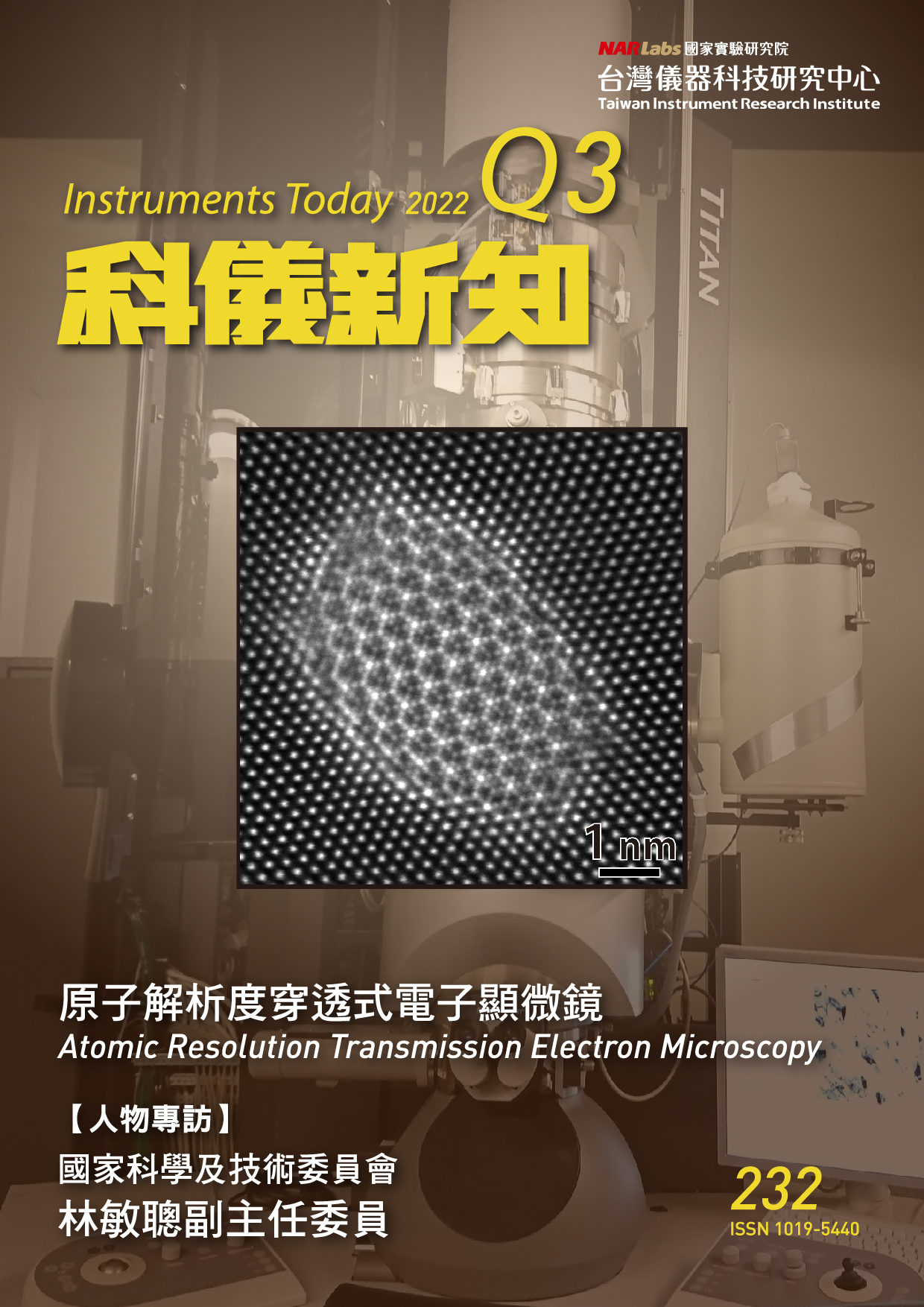
原子解析度穿透式電子顯微鏡
「原子解析度穿透式電子顯微鏡」專題介紹 [ 下載 PDF ]
蕭健男
前瞻研究與新材料開發取決於儀器設備在原子尺度之量測與製程能力。穿透式電子顯微鏡 (transmission electron microscopy, TEM) 可同時得到材料顯微結構 (microstructure) 之形貌、 成份與晶體結構等訊息,並與製程及性質聯結,為重要分析儀器之一。 近年來,隨著高速電腦與影像偵測器之發展,電子光學像差修正與相位回復技術得以實現,並將掃描穿透式電子顯微鏡 (STEM) 之點解析度 (point resolution) 推升至次埃 (Sub-Å) 尺 度。除此之外、STEM 於 X 射線能量散布分析儀 (EDS) 及電子能量損失譜儀 (EELS) 成份分析、臨場 (in-situ) 觀察、4D STEM、三維原子級電子斷層術 (electron tomography) 與搭配原子針尖斷層影像儀 (atom probe tomography, APT) 等技術亦有長足之進展。
緣此,本期以「原子解析度穿透式電子顯微鏡」作為專題,內容包含目前最先進之 STEM 技術與應用發展,諸如「材料原子尺度臨場穿透式電子顯微鏡觀察」、「三維原子級電子斷層顯微技術在半導體元件之應用」、「原子針尖斷層影像儀之半導體元件分析應用」 等文章。「原子級解析七系列鋁合金奈米析出物顯微結構演化之回顧」一文,則是歸納國防航太級七系列 (Al-Zn-Mg-Cu) 鋁合金析出硬化相變態 η 析出物之原子結構解析。「以高解析穿透式電子顯微鏡搭配電子能量損失譜儀重構元素電子、鍵結、成分空間分布」係以 STEM 結合電子能量損失譜儀,同時進行材料原子結構與元素量化分析。此外,「淺談 TEM 分析上常見的主要困惑」為作者整合長年經驗,說明以 TEM/STEM 進行材料分析時所常遇的困 擾,以避免誤將背景訊號與雜訊解讀為實際的材料訊息,而造成製程研發之影響。
綜上所述、STEM 整合 EDS 及 EELS,搭配 in-situ 觀察、4D STEM、 electron tomography 與 APT 等先進技術成為分析平台,為探索原子世界的物理化學現象及發展 Å 世 代科學工業技術提供了可能性。期望本期專題在作者群的介紹下,激發讀者們創新的研究想法與方向,擴大並提升本項儀器之應用範疇與檢測技術。
原子級解析七系列鋁合金奈米析出物顯微結構演化之回顧 [ 下載 PDF ]
鍾采甫, 楊侑倫, 蕭健男, 曹正熙, 李威志, 楊哲人
前瞻性高強度七系列 (Al-Zn-Mg-Cu) 鋁合金,經由人工時效熱處理衍生出多型態奈米 η 析出物,透過高解析穿透式電子顯微鏡影像 (HR-TEM) 與高角度環形偵測器之掃描透射電子顯微鏡影像 (Cs-corrected HAADF STEM),進一步解析主要析出相 η1、η2 和 η4 之顯微結構。搭配快速傅立葉轉換法與模擬相對應繞射圖譜,可清楚鑑定析出物與鋁合金基地的晶體方位關係。進一步,透過真實原子布局影像,釐清相對應 (1120)η1、(1010)η2 和 (0001)η4 晶面 上,所呈現 zig-zag、sandwiched 和 six-fold 原子排列結構情況。此外,巨觀下,奈米析出物的形貌、尺寸大小與體積百分率可藉由小角度 X-ray 散射,加以定量分析。微觀角度中,奈米析出物之間的演化,如:GPII zones 或多型態奈米 η 析出物,亦可藉由 sympathetic 成核成長機制,於第二相 AlMn6 界面孕育而出。此外,3D 針尖電子顯微鏡影像重構是未來更能進一步點出傳統以二維投影影像的盲點。然而,高端儀器的重裝備,更需搭配良好的試樣準備與後續影像重構的尖端技術,才能為材料晶體結構演化展開下一個序章。
以高解析穿透式電子顯微鏡搭配電子能量損失譜儀重構元素電 子、鍵結、成份空間分布 [ 下載 PDF ]
楊子逸, 闕郁倫
本文主要介紹電子能量損失譜儀 (EELS) 的工作原理,以及不同能譜區間能提供哪些之資訊,並比較傳統穿透式電子顯微鏡中常用的成份分析工具 X 射線能量散布分析儀 (EDS) 的差異。在成份分析中 EELS 可提供更準確的低原子序元素成份定量,且由元素特徵峰波形的差異可分析成份鍵結方式;此外在較低能量電漿峰區域更能藉此分析區域的電子性質,包含能隙形式、大小以及介電性質差異。最後,本團隊展示應用電子能量損失譜儀解析機制的三個研究,銅奈米線電阻式記憶體、奈米螺旋二硒化鉬陣列鋁離子能量儲存電池陰極充放電機制、鹼金屬摻雜控制銅銦鎵硒薄膜太陽能電池薄膜成長。
材料原子尺度臨場穿透式電子顯微鏡觀察 [ 下載 PDF ]
吳文偉, 曾奕棠, 羅宏洋, 侯安遠, 沈芳君
近年來,隨著材料元件尺度的微縮,新材料的開發以及材料原子尺度之結構對元件性質的影響越來越顯著。原子的排列影響了材料的結晶性、晶界、缺陷⋯,也大大影響其物理性質、機械性質、化學性質。在元素種類的分佈上,將決定了材料的成份、相生成、偏析⋯等,也同樣導致材料特性表現的差異。在材料科學上,很多的實驗結果以及現象的發生過程並不容易得到直接且有力的觀察與解析,因此原子尺度下直接觀察材料在特定的外加因素如電場驅動下的電子傳輸現象、受熱導致原子擴散及晶粒成長等材料動力學問題、施加應力造成差排移動或缺陷產生之結構變化⋯等,將對於材料的特性與結構間的關係提供最直接且可靠的證據。
三維原子級電子斷層顯微技術在半導體元件之應用 [ 下載 PDF ]
彭裕庭, 劉宇倫, 陳健群
在本文中,將會介紹如何利用球面像差修正掃描穿透式電子顯微鏡,對半導體樣品拍攝無任何缺失角度之高角度環形暗場影像,並且將其重建出完整的三維原子級模型,進行三維原子級電子斷層顯微技術。並以鐵電鰭式場效電晶體作為範例,呈現出有別於過去的高角度環形暗場影像只能提供單一方向的平面投影,此技術可以完整的提供樣品內部結構資訊、各原子在整個空間中的位置分布,可以針對三維重建模型的局部進行更多精細的分析應用。透過這項技術觀察到在過去難以分析的樣品內部微結構,例如在空間中的原子級介面粗糙度,這是在沒有三維原子級電子斷層顯微技術下無法觀測到的。透過範例可以了解此技術最新的應用及發展,得知在高階半導體分析檢測中,可藉此技術得到更完整的樣品結構資訊,並觀察到先進半導體元件在其他檢測技術中無法察覺到的細微缺陷。
原子針尖斷層影像儀之半導體元件分析應用 [ 下載 PDF ]
顏鴻威
原子針尖斷層影像儀 (atom probe tomography) 是一種 state-of-art 材料顯微分析技術,能夠解析材料或元件微觀區域的三維原子分佈,它已經被廣泛應用在材料、元件、地質、生物 等物質的顯微分析,其獨特的空間解析度與成份偵測極限使它成為當代微縮、複雜、且立體化半導體元件研發所需之關鍵技術。本文提供原子針尖斷層影像儀之簡單介紹,並以實際案例展示它在半導體元件之應用,最後探討此顯微分析技術在半導體領域的挑戰與未來發展, 期待提供讀者與半導體領域專家對原子針尖斷層影像儀有更清楚的輪廓與認知。
淺談 TEM 分析上常見的主要困惑 [ 下載 PDF ]
鮑忠興
本文簡短討論幾項在常用的 TEM/STEM 材料分析技術時遇見的典型困擾,包括調機操作,成像技術的選擇,錯誤使用高分辨 TEM 影像,EDS 能譜中銅訊號真偽的判斷,和 TEM 模式的 EELS 元素映像技術等。
科儀專欄
適用於大生物樣本之大口徑顯微物鏡開發 [ 下載 PDF ]
彭偉捷, 陳志文, 陳銘福
層光螢光顯微技術可提供動態的三維空間高解析成像,為目前應用於生物醫學檢測的重要技術,近年來以層光螢光顯微術進行全腦取像更是對於腦神經科學的重大應用。由於傳統商用物鏡的視場角限制,目前仍需要進行影像拼接以觀測高解析大型生物樣本;然而移動物鏡進行拼接相當耗時,且圖像產生拼接痕跡亦造成圖像不連續與解析度下降等問題。因此客製一個大視場的顯微物鏡是取得高解析完整影像的必要方式,以本計畫的物鏡需求規格而言,須具備寬視場 Φ22 mm 可完整拍攝鼠腦影像,以及工作距離大於 30 mm 以針對大型生物樣本作完整深度掃描,更重要的是解析度須達 1 μm 以觀察活體細胞結構。由於大視場的因素,場平坦度與縱向色差的修正更是具挑戰性;超低色散材料搭配消色差膠合鏡應用於物鏡系統的設計與製作,以有效校正縱向色差。其相關光學設計、光機設計與光學檢測等均詳述於本文中。