2003 年 4 月出版
科儀新知 第 133 期
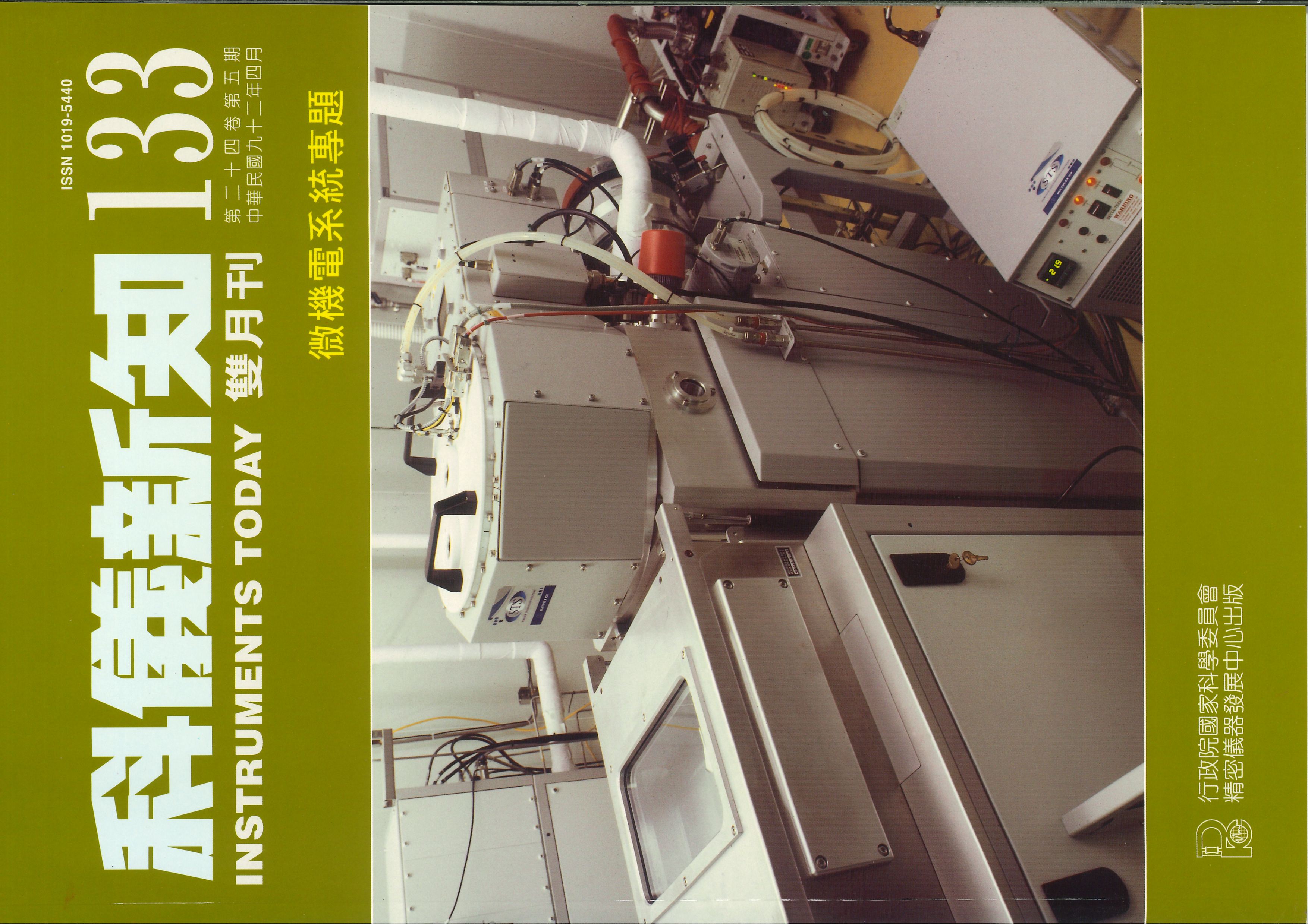
微機電系統專題
微機電製程技術於光開關製作之應用 [ 下載 PDF ]
楊啟榮, 陳柏穎, 趙俊傑
由於 21 世紀網際網路服務的超快速成長與多媒體化,人類已進入多媒體視訊圖像為主的寬頻傳輸時代,使得數據傳輸量的需求與日俱增,如何有效率地倍增網路傳輸容量已成為重要課題。透過微機電製程技術已實現將光開關微小化、積體化及陣列化的目標,並達到降低成本的批次量產能力。本文首先針對各種不同微光開關特性及應用加以比較,接著說明微機電製程於光開關製作之應用實例,最後再指出光開關適用性之基本評估要點。
SU-8 光阻在高解析 X 光微加工技術的新應用 [ 下載 PDF ]
許博淵, 洪瑞堂, 黃泰源, 劉昆沛, 周長彬
本文主要探討以 SU-8 作為高感光對比 X 光光阻的可行性。研究結果顯示,SU-8 對 X 光的敏感度為傳統 PMMA 光阻的百倍以上,而且其光刻側壁表面品質 (Ra ∼ 12 nm) 與 PMMA 一樣優異。本研究亦發現,SU-8 也具有極高的感光對比,亦即所需的光罩吸收體厚度將可有效降低。當光罩厚度夠薄時,便可以傳統的 UV 光刻製作高解析度的 X 光光罩,而不必先製作中間光罩,再藉由軟 X 光翻製較厚的光罩結構。因此,高解析 X 光鼓膜光罩製程將可大幅簡化,具有次微米解析力的 X 光微加工技術在微光學元件的應用潛力將可大幅提升。
微感測器技術於土木檢測之應用 [ 下載 PDF ]
楊龍杰, 吳政忠
微型感測器技術在本文中被用以偵測鋼珠撞擊之..時間原點..;該 6 mm 直徑之撞擊鋼珠,係在混凝土結構表面激發出頻率 100 kHz 以上之暫態彈性波,以便進行土木結構裂縫之非破壞性測定。主動鋼珠撞擊「時間原點」之界定,可精進手提式超音波非破壞性檢測系統之性能。微型壓阻式感測器與鋼珠的封裝方式,以及撞擊訊號量測問題,將在文中一一描述。
微系統封裝技術之介紹 [ 下載 PDF ]
黃榮堂, 陳俊賢, 林夆融, 彭成鑑
微機電系統封裝是指將裝置中的核心結構體組合起來的意思,封裝 (package) 的作用在於保護脆弱的微機電元件 (如感測器或致動器) 免於受外在環境的侵害 (如機械外力或污染等),並負起機械支撐與訊號輸入和輸出的責任。文中將對封裝設計的概要、感測器封裝的特點、各種常見的低階封裝技術與晶圓級多層封裝等作一介紹。
Fabry-Perot 型式抗反射層鍍膜在深紫外光微影二元式光罩上之應用 [ 下載 PDF ]
陳學禮, 鄭旭君
在本文中筆者以 Fabry-Perot 結構的概念,設計了應用於深紫外光微影二元式光罩的抗反射層結構。此抗反射層結構是由金屬/氧化物/金屬三層膜堆所組成。藉由對此結構作最佳化,在波長 248 nm 與 193 nm 的反射率皆可達到小於 1.5% 的水準。在此三層式的 Fabry-Perot 結構中,底層的鉻膜提供了適當的吸收。藉由控制中間的二氧化矽層,我們可以將欲曝光波長的反射率調至最低。而最上層的金屬膜則可避免因電子束直寫所導致的電荷累積效應。
全反射原理及在生物螢光顯微鏡之應用 [ 下載 PDF ]
楊德明, 林夏玉, 蔡定平
隨著活體螢光染色技術如綠螢光蛋白、以及光學技術的快速進展,生物螢光顯微鏡的發展與應用已到達一個成熟而多樣的地步,生物螢光顯微鏡學已成為一個熱門且實用的實驗工具。本文將介紹一種另類螢光顯微鏡-全反射式螢光顯微鏡,其工作原理是利用全反射時所產生的消散波作為螢光激發光源,強調只激發樣品表面螢光分子的特性,加上高解析的物鏡搭配,這類顯微鏡在表面材料科學以及生物學,特別是單一分子偵測的應用上,逐漸受到重視。這類顯微鏡的架構以及生物學上的相關應用等也將在本文中詳述。
植被及國土變遷觀測儀 B2 幾何精度評估 [ 下載 PDF ]
林修國, 黃鼎名
本文介紹國科會精密儀器發展中心研製的機載遙測儀器-植被及國土變遷觀測儀綠光波段 Band 2 幾何校正的過程,並比較實際機載影像產生之正射影像與地面已知座標的點位,評估其正射影像精度,以中央 1 個及外圍 5 個點位為控制點進行座標轉換,得到控制點的均方根誤差 RMS 為 0.51 像元 (換算地表的精度約為 25.7 公分),另以其餘 8 個點位為檢核點得到 X 軸的 RMS 為 0.74 像元 (37.5 公分),Y 軸的 RMS 為 0.45 像元 (22.6 公分)。
談光學標準尺的校正方法 [ 下載 PDF ]
何傑
光學標準尺亦稱玻璃尺,是一般精密儀器如三次元量床或工作母機之重要定位組件,亦可當作長度標準進行直接量測,或使用在投影儀與工具顯微鏡的校正工作上。光學標準尺的形式一般為石英玻璃所製,上有極細之刻線。其校正原理係利用精密雙軸量測顯微鏡之工作平台為載具,將光學標準尺置於其上,以雷射干涉儀為標準,與光學標準尺移動之距離進行比對。鑒於一般讀者對光學標準尺的了解機會不多,而且由於品質認證工作的推行,光學尺的校正工作日益重要,因此特撰此文,增加讀者對此方面之了解,且希望本文能對從事長度校正工作之人員提供參考。
電子鼻技術簡介 [ 下載 PDF ]
吳仁彰
由於多用途及快速分析樣品的需求日益迫切,電子鼻也成為日漸普遍的分析儀器。本文以分段介紹方式,敘述電子鼻、嗅覺及氣味分子感知原理、電子鼻技術的發展歷史、電子鼻感測原理、國內外發展情況及未來發展趨勢等,以期對電子鼻技術有興趣者有所助益。